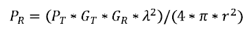
Astronaut-Lander Link
The link between the astronaut and the lander must support high data rates for audio/video transmissions from the astronaut to the lander.
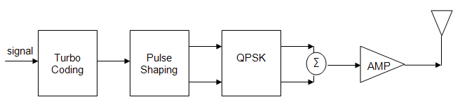
The link from the astronaut to the lander is depicted in the figure below:
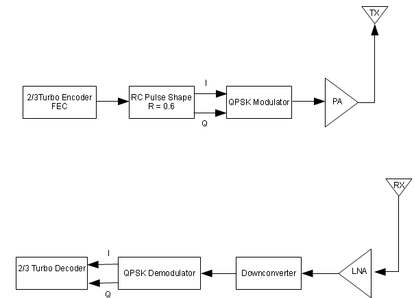
Figure 1. Uplink and downlink functional block diagram
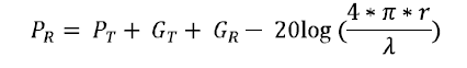
The system will utilize the same ¼ wave monopole omni-directional antenna on the lander as well as on the astronauts CommPak. The antenna was tested in an anechoic chamber at Carnegie Mellon University. The antenna was fine tuned for a carrier frequency of 2.45 GHz and was found to have a gain of approximately 32 dBi. The S11 plot, rectangular and polar gain plots follow:
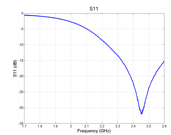
Figure 2. Return loss fine tuned for minimum loss at 2.45 GHz carrier frequency
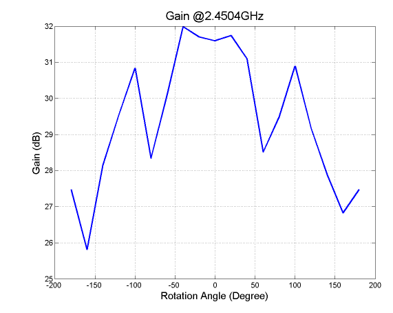
Figure 3. Rectangular gain plot displays a max gain of 32 dBi
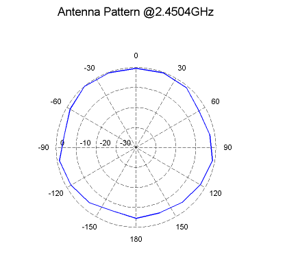
Figure 4. Polar gain plot displays directivity of rf power
From the S11 plot, we can further estimate our RF bandwidth to be approximately 100MHz at |S11|< -20 dB for a return loss of 1%.
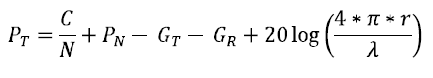
The link budget will be calculated at worst case, transmission at day time when the temperature on the surface of the moon can get as high as 380K (106 degrees C). At this temperature, electronic thermal noise contributes very little to the total system noise. The antennas ambient temperature becomes the greatest contributor to system AWGN, additive white Gaussian noise. The noise power can be estimated to be:
Where TPHY is the ambient temperature on the surface of the moon at day time, 380K. The design is to achieve a CNR as close to the Shannon limit as possible with a relatively low transmit power from the astronauts CommPak. The goal is to minimize load on the Lithium-ion battery packs providing the range of 2.5 km or greater from the lander.
Before we calculate the optimum carrier to noise ratio we must realize that we are using the same antenna for transmit (astronauts antenna) as well as receive (landers antenna) and this will limit us to fitting all data within a 100MHz band.
We receive a compressed MPEG-4 data stream of 1.5 Mbit/s from a digital camera. This data must be transmitted to the lander on a 2.45 GHz carrier frequency where it is logged for scientific study. We modulate the data signal with a π/4 QPSK modulator and encode with a 2/3 Turbo encoder for forward error correction. We must band limit our transmit signal to avoid inter-symbol interference criterion with a RRC bandpass filter with a rolloff factor of 0.6. The information presented to this point is summarized in the table below:
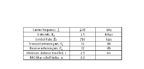
Design specifications
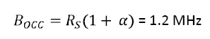
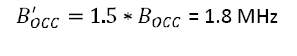
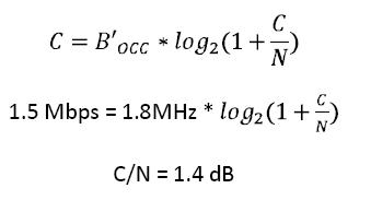
Solving for C/N we find that, theoretically, only 1.4 dB of carrier-to-noise ratio will be needed to achieve this data rate. The design will try for a carrier-to-noise ratio of 20 dB so that near perfect transmission is more probable.
The transmit power must be minimized such that the battery power sources are not exhausted too rapidly. The following calculations are to obtain the power level needed at the astronaut's transmit to achieve a link between the astronaut and the lander.
LINK BUDGET ASTRONAUT TO RFID TAG
The link between the astronaut and a RFID tag will be used to navigate the astronaut safely back to his lander.
This link is a backscatter link, where the transmitting antenna on the astronaut's CommPak must first excite the tag for an 8-bit tag id to be
sent to the astronaut. In this document, the link between the astronaut and the RFID tag is characterized.
The antenna used to communicate to a RFID is the UL-9150-360, a 1 GHz custom tuned antenna created by www.antennas.us.
The link is depicted in the figure below:
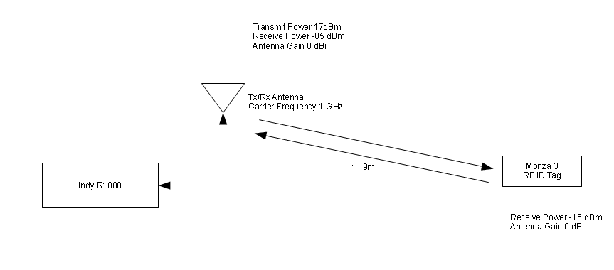
Astronaut RFID Link
The information in the diagram above is summarized in the table below:

Design specifications of astronaut to RFID tag link
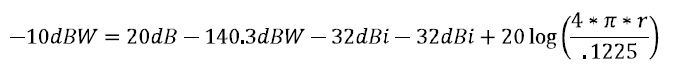
We would like to be able to receive a signal 9 m away from the RFID tag. Using a simplified monostatic backscatter link equation,
we can calculate the maximum distance at which a backscatter signal can be detected. The calculations follow:
Solving for r, we get 8.47 m as the maximum distance that we can detect a signal from the tag.
Modulation
One of the key points of our design is the definition of a proper modulation and coding scheme.
To define such devices, we have to keep in mind the specifications
that have been set. We are allowed to work in a bandwidth between 1 and 3 GHz, also we do not
have a specific required power for these kinds of devices. However, we are constrained by the
amount of power the batteries can supply.
The RFID-to-astronaut modulation scheme is handled by the Indy R1000 reader chip. It uses ASK.
Astronaut-to-Lander Modulation
A transmission link that we have to design is the one between the lander and the astronaut.
Since both devices are active, we can use a modulation scheme that requires more power. Although QPSK modulation
requires more power, it will allow us to transfer data at higher rates. Unlike the breadcrumbs, the
astronaut-to-lander link will have higher data rates to support video transmission. Another positive
aspect of this modulation is the robustness against amplitude modulation distortion. This capability
is important to avoid bit errors due to the hostile surface of the moon. A more complex modulation scheme
could be used, (e.g. 16-QAM) but a higher bit error rate would occur.
We have chosen a device from the MITEQ company, in particular, a QPSK modulator (SDM0104LC1MDQ) that
has a frequency range between 1 and 4 GHz with a typical required power of 10 dBm. This device will
help us meet our specifications with small power requirements. Also, this device is approximately 6 cm x
4 cm x 1 cm. This size allows us to make the electronics that the astronaut has to bring very
compact and easy to carry along.
We have to design a pulse shape that will keep additive frequencies from spreading into
the near bands. Due to the addition of the turbo coder, our rate will be 2.25 Mbps, using a
roll-off of 0.6. The pulse shape is shown below.
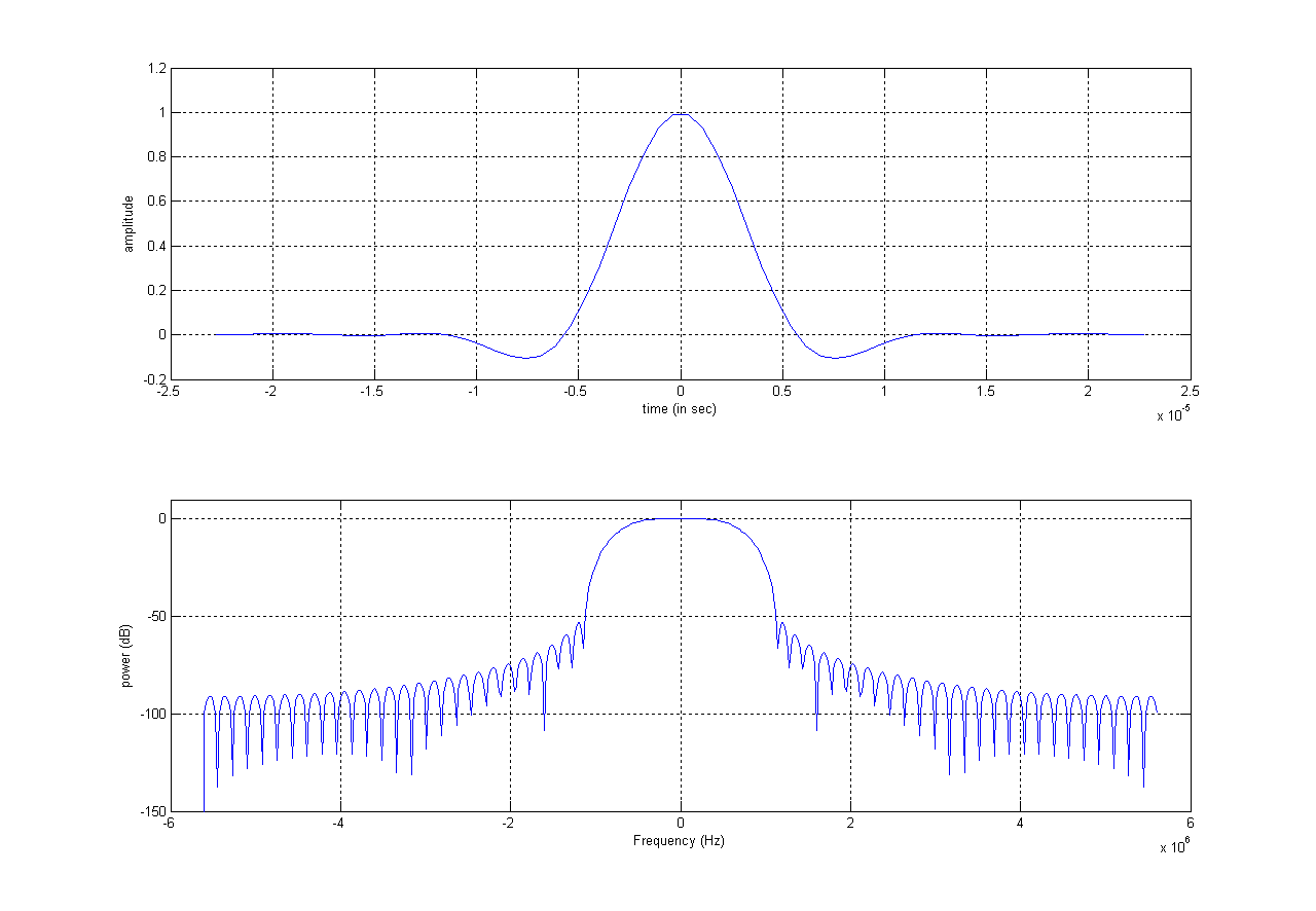
Pulse shaping for 2.25 Mbps
The last device in our chain is the power amplifier. We will use a LNA/power amplifier made by AVAGO (MGA-24106). The specifications include a gain of almost 18 dB, a very low noise figure of about 0.91, and a required power of 13 dBm. Finally, we are using a turbo code as the error correction coding in order to provide high reliability in the transmission. It will help us to increase the performance close to the Shannon limit.
Block diagram of the link between the Atronaut and the Lander.
RFID TAG AND READER
RFID TAG DESIGN
The front part of our RFID Tag design would have our company Logo.
The back part of our RFID Tag design would have the etched antenna and the RFID Chip.
OVERVIEW
Once the Astronaut has come out of the lander and is ready to explore the lunar surface, he would have a handful of RFID tags with him. The astronaut drops the RFID tag and simultaneously excites the previously dropped RFID tags to obtain the (x,y) coordinates of the current RFID tag. The location is determined using a three antenna design that utilizes signal strength and angle of arrival measurements with respect to the previous RFID tags. Meanwhile, as the calculations of the (x,y) coordinates of the current RFID tag is going on, the reader excites the current RFID tag which is to be dropped to obtain its tag bits. On demodulating the current tag bits, the tag bits and the corresponding x-y position are stored in the Cypress PSoC flash memory. An RFID tag will be dropped whenever the astronaut is about to move out of line-of-sight or the signal strength degrades past a certain level. We have determined this distance to be approximately 8-9 meters.
Our RFID tag would be manufactured by a company called Impinj which manufactures RFID tags for industrial and commercial purposes.
These RFID tags would be tuned by the manufacturers for a special frequency of 1 GHz due to the absence of the FCC rules on the moon.
This RFID tag would be passive and would be programmed with an 8 bit RFID tag number which would help in decoding the coordinates from the flash memory.
The RFID tag would also have an anti-collision protocol in them which would prevent many excited passive RFID tags to transmit at the same time.
The main purpose of the RFID tag is, whenever excited with a power of around -20 dBm, to transmit its tag number to the RFID reader which would decode
it and display the (x,y) coordinates on the LCD Screen through the Cypress PSoC. Such types of passive RFID tags are available for a relatively low cost in the market at
around $1.20 dollars apiece. They have an antenna which improves the reading range of the tags.
The PSoC Kit which would be used for displaying (x,y) coordinates.
Basic Operation
RFID Tag
A passive RFID does not have any batteries. It derives its power from the carrier wave which is transmitted by the reader. With the help of this power, the passive RFID tag would transmit its stored bit pattern by switching between a set of impedances. The tag will switch to the smaller value of impedance to transmit a 1 and a higher value of impedance when transmitting a bit 0. This transmission scheme results in Amplitude Shift Keying. The amplitude variations of the transmitted wave contain the bit pattern. This signal can easily be decoded with the help of a simple peak detector.
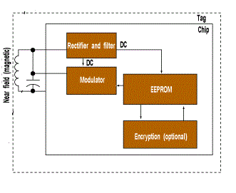
Block Diagram of a RFID Tag chip.
Monza RFID Tag

Monza 3 Tag RFID Chip with Thin Propeller antenna design.
The internal circuit block diagram of the RFID Monza Chip from Impinj is as follows:
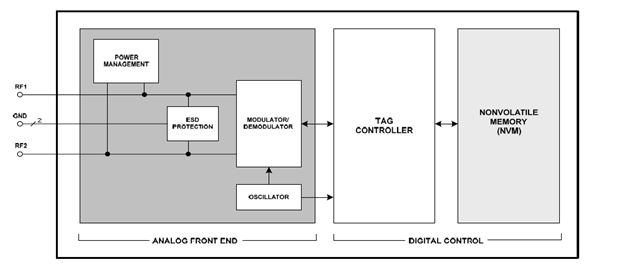
Internal block diagram of the Monza RFID tag.
We have the option of connecting two antennas, but in our case we have grounded the terminal of the second antenna and have used the Thin Propeller
etched antenna design by Impinj, as it is well-suited for long-range applications.
Power Management
The RFID tag receives the power from the carrier wave generated from the active reader. The power management block converts the received RF power into a DC Voltage that excites the chip. The power management block is a simple diode rectifier which gives a stable DC output voltage.
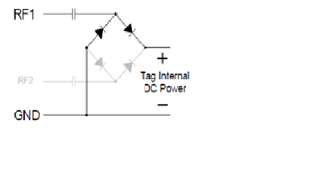
Internal Diagram of the Power Management Block
ESD Protection
ESD protection blocks the shunt charge from the positive and negative sources, protecting the RFID tag from being damaged in case it receives an excess amount of power.
Antenna Design
The thin propeller antenna design by Impinj, is a specially designed antenna to be used with Monza RFID tag for long range applications. It increases the range and the read sensitivity to around -15 dBm. The antenna design is shown below:
Modulator Demodulator
This block demodulates the carrier signal from the reader, the main purpose of demodulating a carrier wave from RF Reader would be used in
access passwords. Demodulator would not be of much use here as we do not intend to send any information in the carrier wave from the reader to the tag.
In case of the reverse link from tag-to-reader, the modulator would switch between two impedances having a reflection coefficient of about 0.8 to modulate
the RFID tag bits in ASK. The line encoding would be done in FM0.
Modulation
In passive RFID tags, there is switching between the two different impedances values for transmission of bit 1 and bit 0 and it results in amplitude
modulation. Therefore, the modulation used in the communication between the RFID tag and the reader link is ASK.
Non Volatile Memory
Non-Volatile Memory is divided into two sections:
1. EPC Memory
2. Reserved Memory.
We have opted for no reserved memory, as we would need only 8 bits of the EPC memory for our RFID tag bits. This EPC memory is field programmable.
Anti-Collision Protocol
If more than one RFID tag becomes active and transmits the RFID tag bits, it would lead to collision at the reader end and hence the reader would not
be able to properly decode the information being sent to it. To counteract this problem, the tag has a protocol which has a random number generator
and the tag would wait until a small random time and then retransmit the bits to the reader.
EPC Memory
The EPC memory contains the CRC, protocol bits, and the RFID tag value of the respective RFID tag and is field programmable.
Forward Link Characteristics
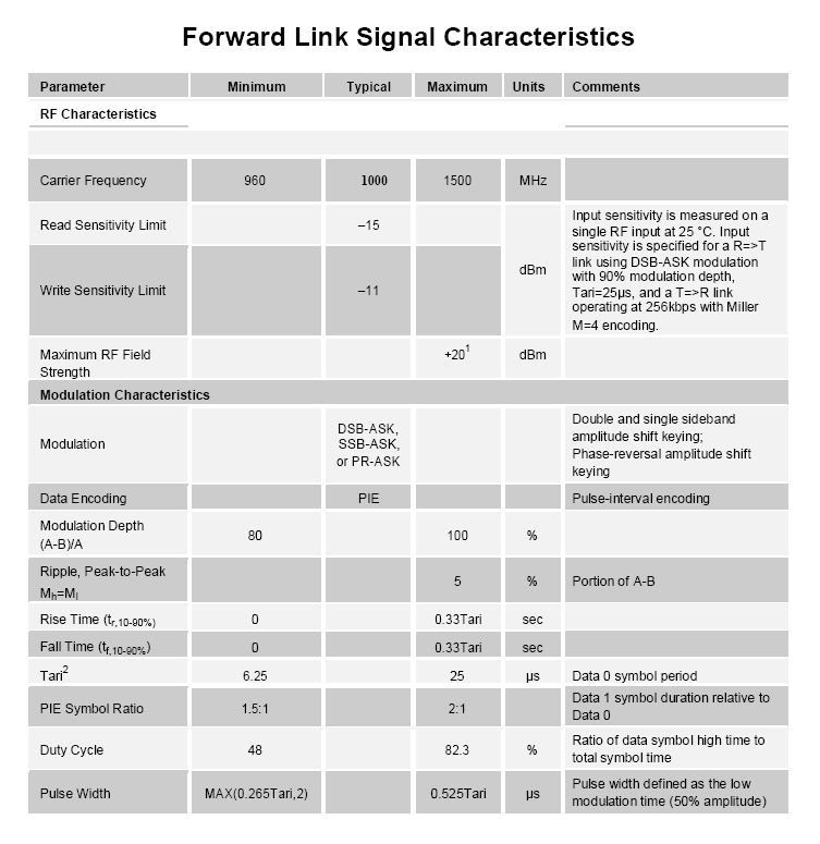
Reverse Link Characteristics
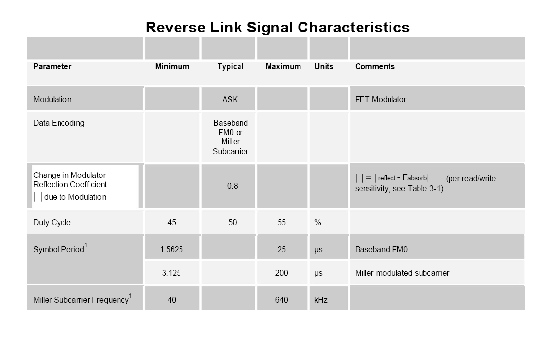
Internal Circuitry, the Forward Link, and Reverse Link characteristics are taken from the datasheet of the Monza 3 tag chip.
RFID Reader
The RFID reader is a device which transmits the power waves at a chosen frequency to excite the passive RFID tags within the calculated range.
The simple block diagram of a RFID reader is shown below:
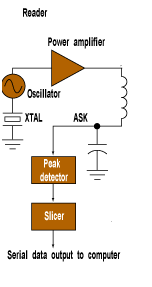
Block Diagram of the Reader
The waves produced by the oscillator are amplified to increase the range, thereby getting data from more RFID tags. The amplitude modulated (ASK)
data transmitted by the excited RFID tags, is demodulated by a simple peak detector in the reader and sent to the PSoC kit for mapping the
(x,y) coordinates and displaying it on the LCD screen.
We have used the Impinj Indy R1000 Reader chip connected to an antenna for our reader. This IC would be placed onto the fixed breadboard
connection on the PSoC kit and it would be securely connected.
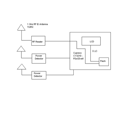
Block Diagram of the Reader module.
Space Protection
The temperature on the moon is very different from the earth, hence most of the electronic items are non-functional on the moon.
The temperature on the moon varies from -153 degrees Celsius at night to +107 degrees Celsius during the day.
No electronic component would be able to survive such high and low temperatures.
The RFID tags would be exposed to such temperature and in order to protect them, the etched part would be covered with multi-layer insulation
which is produced by General Dynamics. Therefore, the RFID Chips would be protected from the harsh temperature. Due to the insulation,
the temperature inside the thermal blankets would be in the operating range.
The RFID reader inside the astronauts suit will not require additional protection.